A first look at the basics of RF shielding.

At the most basic level all electrical circuits have an electric and magnetic component (E&M fields) associated with them. This includes the cables, the wire traces, components, and physical enclosures that make up the circuit. These E&M fields can interact with each other and cause undesired effects between components. As an example, a transformer uses magnetic fields to convert one voltage to another voltage to power a circuit, but the same magnetic field if not properly shielded may induce an interference into a signal cable that is not properly routed.
Describing RF shielding will require mixing some terminology from E&M fields and their Lumped Element Model (LEM) equivalents using capacitors (Electric Fields), inductors (Magnetic Fields), and resistors (energy dissipation).
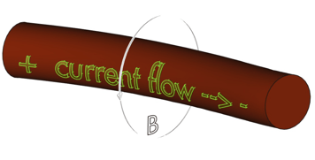
In its most simple configuration, a conductor carrying an electric current has a magnetic field (B) associated with it when a potential difference (voltage) is applied between the ends.
|
| Magnetic Field 'B' around a Conductor |
The magnetic field spreads outward and curls around the conductor following the right-hand rule. The right-hand thumb point in the direction of current flow and the fingers wrapped around the conductor point in the direction of the magnetic field.
At the same time the conductor is surrounded by an electric field (E) that is generated from an external source such as a battery, an AC supply, or a signal generator. It is this electric field that transfers energy from the external source to the various elements in the circuit made up of resistors, capacitors, and inductors.
The shape of the electric field depends on the physical characteristics and dimensions of the conductor and circuit elements. Energy transfer can occur even if the circuit is not ‘closed’, the circuit behaves like an antenna and can generate electromagnetic interference (EMI) or pick up electromagnetic compatibility (EMC) fields.
An interesting thing to point out is that current flow is opposite to the direction that electrons in the conductor travel. Additionally, only a small fraction of the electrons in a conductor are available for current to ‘flow’, the large majority are moving in random directions due to thermal effects.
In the case of a battery powering a copper conductor circuit, the electrons are moving at a rate of less than 0.025mm/sec from the negative terminal to the positive terminal of the battery…an extremely slow rate! When we look at a 60 Hz alternating current, the electrons are moving back and forth over a distance of only 0.2 micrometers. At microwave frequencies the electrons move less than the width of a copper conductor nucleus.
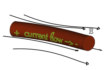 |
| Electric Field 'E' around a Conductor |
The energy transfer from a battery, AC source, or a signal generator is done by the interaction of the electric and magnetic fields with the electrons (current flow) around the circuit. This picture of a circuit gives a way of looking at how RF shielding can be used to reduce EMI and EMC.
The purpose of RF shielding is to control how the electric and magnetic fields are distributed and to prevent unwanted behavior in the operation of a circuit. A simple way of controlling the fields is with the use of shielded conductive compartments on a PCB.
The RF shield is used to control the electric and magnetic fields from interacting between the different parts of the circuit by keeping them confined to specific areas.
The enclosure has grooved slots fitted with a conductive gasket around each compartment to make sure there is a continuous electrical contact with the corresponding PCB.
All machined metal covers have some roughness and gaps when two surfaces are in contact with each other. The gaps are comparable with the distance that electrons can travel when excited by AC currents or signal generators. The electric and magnetic fields can ‘leak’ through the gaps and cause unwanted signal degradation.
RF shields can also be placed over sensitive areas of a circuit when other parts of the circuit are well laid-out.
For more information on RF shielding, stay tuned for part 2 or please contact Averna.
--
By Peter Barabas
Senior Test Specialist - Engineering & Consulting
![]()
You may also be interested in…

Are you struggling with RF testing? You’re not alone. Read our eBook for tips to tackle them!
Get in touch with our experts or navigate through our resource center