This post will attempt to cover many key aspects of creating modular LVFPGA code. This can be a very lengthy topic. Instead of trying to create a single all-inclusive post, this one will cover some high level basics. Future posts will go deeper into important topics. If you have comments or questions, be sure to post them at the bottom of this blog.
FPGA projects can tend to be lengthy battles of resource minimization, timing optimization, and algorithm performance. Getting a function just right requires varying degrees of art, experience, process, and science. Once it is complete, it's time to celebrate. But then the next project brings its own combination of new and old challenges. If we plan, we can limit our need to rehash old challenges.
Code reuse is common with any type of development, from database to user interface to hardware programming. Each has its own best practices to ensure minimal rework. When deriving the best practices for LVFPGA, we must be sure to consider the following aspects:
- Algorithm data flow, inputs and outputs
- Algorithm configuration
- API/UI
- Unit Testing
- Distribution
Moving Around Your Data
Most algorithms need to get data in and/or out. Moving an algorithm from one project to the next works best if standards are followed. The three most common ways to pass data in/out of a modular block are through:
- FIFOs: pass in FIFO references for input (read inside module) and output (write inside module)
- 2-wire handshake: 'data valid in' and 'data valid out'
- 4-wire handshake: additional flow control signals
Deciding which option to choose is not only affected by the design of this module but also the environment in which this module might operate. For instance, if your definition of modularity includes being able to move this algorithm to other clock domains or even other FPGA boards, a FIFO might make the most sense. Another situation where a FIFO might make sense is if the algorithm has a specific data flow requirement, for instance batch processes. While FIFO's add module location flexibility and processing rate flexibility, they come at a cost of complexity, resource usage, and latency. They should only be used if necessary.
A much lighter weight option is the 2-wire handshake protocol. In this arrangement, data is paired with a 'data valid' boolean line. The algorithm is active on clocks with valid data and not when there is no data to process. Likewise if the algorithm produces valid data on a clock, it sets the 'data valid out' wire to true to signal downstream modules. This is the simplest of interfaces to implement. It is limited in that it cannot control the flow of data. While that might not be important for this block, it might be for one downstream. Imagine the situation where there are three blocks being connected. The first block produces data, the second (our modular algorithm) performs some process on the data, the final block outputs the data. If the output block needs to control the rate of data by applying back pressure, it has no way to do so with our 2-wire module. Instead it will have to apply back pressure to the source but account for the pipeline length in the 2-wire module. This requires extra logic/buffering in the output module.
The best compromise is the 4-wire handshake. This adds flow control to the module which adjacent modules can use. If they are not needed, they can be wired to constants.
Algorithm Configuration
Having separate top-level front panel controls for the configuration of each algorithm is messy and a huge waste of FPGA resources. National Instruments (NI) has created standard methods for using a DMA channel to send data to the FPGA in a safe and efficient manner. The two main methods are:
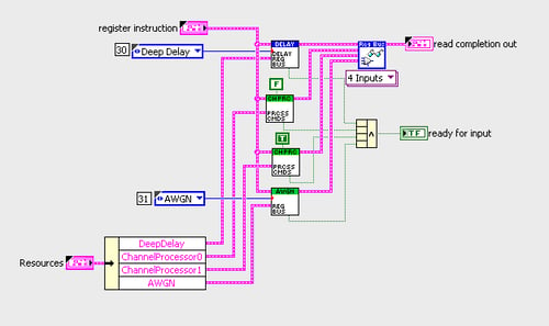
In both of these instances, NI exposes data instructions to the FPGA on a clock by clock basis with a FIFO like access. A single bus can be shared by many modules. As a module creator, there are 4 main FPGA components to develop:
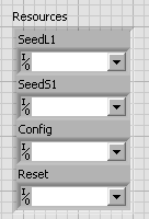
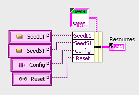
- A Typedef containing a cluster of all resources used by the module

- A VI that does a local instantiation of all these resources

- A VI that accepts data from the instruction bus and makes updates to module resources

- The module algorithm (main processing code)
A module's resources can be made up of FIFOs (local or DMA), memories (BRAMs, DRAMs, etc.) and registers (simple or handshake). For most typical situation registers will be the common choice. When creating a register, decide how that configuration element might be used before choosing between simple and handshake. Handshake requires additional processing but can be much safer in many dynamic cases. There is a lot of discussion on the NI Forums. Perhaps the most concise is here (although minimize use of target scoped resources to improve modularity).
API/UI
Writing a complete module involves not only getting the FPGA code working correctly but also making it accessible from the host application. User interfaces can change from project to project. A module designer should focus more on accessors to configuration and data and less on UI components as they will change from project-to-project. The API should expose all functionality. It can be formatted in a library, class, or any other typical method that aligns with your company's current best practices. The one important rule to follow is to always use dynamic FPGA Interface References. Consider a complete FPGA bitfile to be a collection of modules. These modules have no knowledge (barring special circumstances) of other modules on the bitfile. By using dynamic FPGA interface references it allows all modules to share the FPGA reference without knowledge of other modules datatypes. In each of the API's subVIs there is a call to a 'Dynamic FPGA Interface Cast'. There are two options here based on a company's best practice. One is to configure the reference type to contain just the resources needed by this particular API call. The second is to create a typedef for this module that contains all the module's resources in a single FPGA reference constant and use this with the cast. Regardless of method, using the dynamic FPGA interface reference assures modularity.
Unit Testing
To me unit testing is the most important, most overlooked, task in module development. The way a module will see data and configuration changes on the FPGA can be complex. Testing the code to work in every scenario is the only way to ensure your module will not cause headaches now or on future projects. By using certain rules on the interface (like the 4-wire handshake) and testing a module in every type of worst case scenario is crucial to reducing integration testing time. For large projects, integration testing can take a very large percentage of the entire project's duration and has huge impacts on schedule. The best way to minimize integration testing time and risk is through proper planning and architecture and very thorough unit and assembly level testing. The topic of unit testing is very important and large. Future blogs will go into more details on this topic. For the modularity discussion it is important to make sure that not only thorough unit testing is performed but that the tests are written to allow them to work in various assembly level testing as well.
Distribution
Distribution takes on difference forms based on how far it is being distributed. For instance, the packaging could be different for a company local reuse as opposed to distributing modules a 3rd party solutions. This type of distribution differs from a final application distribution because future compiles will be required against this code. This limits what can be done with it. Simple best practices include:
- Keep your module in a dedicated folder
- Create a project at top-level to contain your FPGA Targets and your libraries of code
- Use separate sub-folders and libraries for FPGA, Host, Shared, and Testing VIs
- Include documentation and/or example code
Optional considerations are creating packed libraries for API code and also using a package manager (i.e. NI or JKI) to simplify distribution as a 3rd party add-on.
