Key Takeaways: What You will Learn About PCBs and PCBA Testing
► PCBA testing is essential to catch defects like shorts and misalignments before final product integration, preventing failures and safety risks.► Multiple testing methods, including AOI, X-ray, ICT, and FCT, ensure quality and reliability across different board complexities.
► Miniaturization challenges are driving the adoption of flexible solutions like fly probe testing and vision inspection systems.
► Automated test equipment (ATE) boosts speed and accuracy. Platforms like Averna’s UniLine enables scalable, multi-test integration for diverse product lines.
Printed Circuit Boards (PCBs) are the backbone of modern electronics, powering everything from smartphones to spacecrafts. As electronics become smaller and more complex, ensuring the reliability of PCBs through rigorous testing is crucial.
What is a PCB?
A Printed Circuit Board (PCB) mechanically supports and electrically connects electronic components using conductive tracks, pads, and other features etched from copper sheets laminated onto a non-conductive substrate. They simplify and standardize electronic circuit design, allowing consistent integration of components.
What are the Three Main Types of PCBs?
- Single-sided: These boards have conductive copper and components mounted on one side. They're used in simple electronics like LED panels.
- Double-sided: Conductive copper layers and components are mounted on both sides, connected via vias They are designed for more complex devices like power supplies or radios.
- Multi-layer boards: These stack multiple PCB layers and are separated by insulating layers. They support high-density and high-speed designs like smartphones, computers, and aerospace systems.
.jpeg?width=400&height=211&name=Vision-inspection-PCB-circuit_AdobeStock_304302934%20(1).jpeg) What Do PCBs Look Like?
What Do PCBs Look Like?
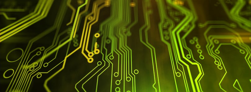
Typically, PCBs are often green due to the solder mask applied for path insulation and copper protection. The boards feature copper tracks, component footprints, vias and sometimes surface markings or labels indicating polarity, component values, or test points.
What is the difference between PCB and PCBA?
PCB refers to the bare board, before any components are added. Once components such as resistors, capacitors, and ICs are soldered onto it, it becomes a Printed Circuit Board Assembly (PCBA). While PCBs are the foundation, PCBAs represent the functional unit ready for integration into electronic devices.
What are Printed Circuit Boards Assemblies Used for?
PCBAs are used across virtually every industry. You’ll find them in consumer electronics like smartphones and TVs, or automotive systems, aerospace navigation, industrial automation, and medical devices. Their applications are diverse, significantly increasing the functionality of different products.
How Does a PCBA Work?
A PCBA works by connecting electronic components using conductive pathways etched from copper sheets. Different signals flow through these tracks to perform desired operations. Components like microcontrollers, diodes, capacitors, etc. interact as programmed and are capable of everything from basic calculations to complex communications.
Why is Printed Circuit Board Assembly Production Testing Important?
PCBA testing ensures that each board performs as expected before it is integrated into a final product. It identifies manufacturing defects such as open circuits, short circuits, misalignments, and faulty solder joints. Without rigorous testing, defective PCBAs can lead to product failures, increased returns and potentially safety hazards.
How Do You Test a PCBA Board?
Testing can be done manually or automatically, depending on the complexity and quantity of boards. Key steps may include visual inspection, component checks and functional verification. As complexity increases, automated test systems become essential for efficiency, consistency, repeatability and quality.
Common PCBA Testing Methods:
Automated Optical Inspection (AOI)
AOI uses high-resolution cameras and lighting systems to inspect PCBAs for visible defects like missing components, soldering faults, and alignment issues. Modern inspection tools utilize 2D and 3D cameras, advanced lighting, and AI-powered software to detect issues. Automated vision inspection equipment verify quality and repeatability of manufacturing process
X-Ray Inspection
X-ray testing allows inspectors to view internal layers or hidden joints, such as those under Ball Grid Arrays (BGAs), revealing solder voids or internal shorts invisible to the naked eye.
In-Circuit Testing (ICT)
In-circuit testing detects shorts, opens, and incorrect component values, typically without powering up the board. This test method requires special PCB design. Access to each component must be included to measure Test Points (TP) and must have a dedicated fixture (bed of nails). That said, this test process is becoming more and more difficult due to miniaturization and higher density.
As an alternative to a bed of nails, a fly probe tester can be used. This is ideal for prototypes or low-volume runs and uses movable probes to test circuits without the need for a custom fixture. Though slower than ICT, it is flexible and cost-effective for initial development.
Functional Testing (FCT)
FCT evaluates whether the PCBA performs as intended, under real-world conditions. Inputs are applied, and outputs are measured to validate the desired response. It is also common to include Flashing or final programming / configuration during FCT.
Burn-in Testing
This stress test powers the board under different environmental conditions (e.g. high temperature or varied electrical parameters) find early failures. It helps ensure long-term reliability, especially for mission-critical applications.
The Future of PCBA Testing
The future lies in smarter, faster, and standardized integrated testing systems. Innovations like AI-driven inspection, predictive maintenance, and modular in-line test systems are reshaping how PCBAs are validated and overall component testing. As devices shrink and become more powerful, test methods are evolving to match the pace of design complexity and production requirements.
Choosing the Right PCBA Testing Equipment
Automated Test Equipment (ATE)
ATE systems automatically perform a wide range of tests, often integrating ICT, FCT, and AOI in one solution. The benefits of ATEs include higher speeds, repeatable accuracy, and reduced human error. This is essential in high-volume production to remain competitive and maintain product quality. Automated test equipment supports various industries and can be customized to match any specification.
Platforms like Averna’s UniLine is an example of an in-line test platform for PCBAs. It offers a flexible approach, integrating various test types (FCT, ICT, AOI, EOL) into a single, scalable platform. This flexibility is especially beneficial for manufacturers producing different product variants on the same line.
Automated PCBA Testing with Averna
As a long-term strategy, automated test systems can reduce non-recurring engineering (NRE) costs by leveraging reusable test cases. This significantly cuts down time and resources needed to launch new products. Averna’s solutions are tailored to a specific customer product ensuring high-quality outcomes across industries.
As PCB technology evolves, so should your testing strategy. Discover how Averna’s advanced automation and vision inspection systems ensure quality and consistency. Contact us for more information!
--

You may also be interested in…
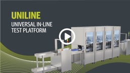
What does the perfect PCB test platform look like? Check out UniLine, the most flexible system on the market.
Get in touch with our experts or navigate through our resource center.