

Most integrated circuits are defined for life the moment they leave manufacturing. A field-programmable gate array (FPGA) works differently.
Key takeaways:
- An FPGA is an integrated circuit whose logic can be reconfigured after manufacturing by loading a configuration file called a bitstream.
- Engineers describe FPGA designs with hardware description languages such as VHDL and Verilog, or with higher-level tools like LabVIEW FPGA.
- FPGAs shorten prototyping cycles for complex designs, including 5G systems that would otherwise require custom silicon.
What is an FPGA? Definition
An FPGA, or field-programmable gate array, is an integrated circuit made of logic cells linked by a programmable routing network. Instead of executing instructions like a processor, it is configured to become a specific digital circuit. In most modern FPGAs, that circuit can be redefined as often as needed after the chip is manufactured.
Each logic cell is a small building block that performs a basic function, such as a simple Boolean operation or storing a single bit. On its own, a cell does very little. Wire thousands of them together through the routing network and they form a complete circuit, whether that is a counter, a communication interface or a signal-processing pipeline. “Gate array” refers to the grid of logic resources laid out on the silicon, and “field-programmable” means the configuration happens on site, by the design team, rather than at the semiconductor foundry.
Is an FPGA Hardware or Software?
An FPGA is hardware whose functionality is defined by a configuration file. Ask an FPGA engineer the question, though, and you’ll get a twenty-minute answer that boils down to “both, unfortunately.”
The chip itself is silicon, with transistors and I/O pins you can probe. But its behavior is defined by a design file that engineers write, simulate, and debug the way they would software. The difference lies in what happens to that file: a processor reads and executes software instructions one by one, while an FPGA never executes its configuration at all. Instead, the file configures the hardware resources inside the device by setting routing switches and lookup tables, and the circuit does the work, with many operations happening on every clock cycle.
How Does FPGA Architecture Work?
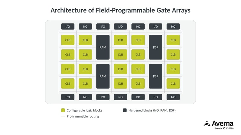
An FPGA is organized as a two-dimensional fabric. When the chip powers up, it loads a configuration file called a bitstream, which defines what each block does and how the blocks connect to one another. That fabric is built from a handful of fundamental elements:
- Configurable logic blocks, built around lookup tables (LUTs). These small memories store the output for every possible combination of inputs. Paired with flip-flops, they can implement combinational functions as well as sequential logic such as counters.
- The programmable routing network, a mesh of wires and switches that connects the blocks to each other. It takes up a large share of the chip and often has the final say on timing performance.
- I/O blocks, which connect the fabric to the outside world and can be configured for the required signaling standard, voltage levels, and interface requirements.
- Hardened resources, including DSP slices for signal processing and block RAM (BRAM) for buffering. Many modern FPGAs also integrate hardened peripherals such as PCIe controllers, Ethernet MACs, complete multi-core processor subsystems, and RF Data Converters (RFDCs).
- Configuration memory, most often volatile SRAM that reloads at every startup. Flash-based devices retain their configuration without power, while antifuse devices, programmable only once, are favored in space applications for their radiation tolerance.
How Is an FPGA Different from a Microcontroller or an ASIC?
FPGAs, microcontrollers and ASICs (Application-Specific Integrated Circuits) are all integrated circuits, but each one serves a different purpose.
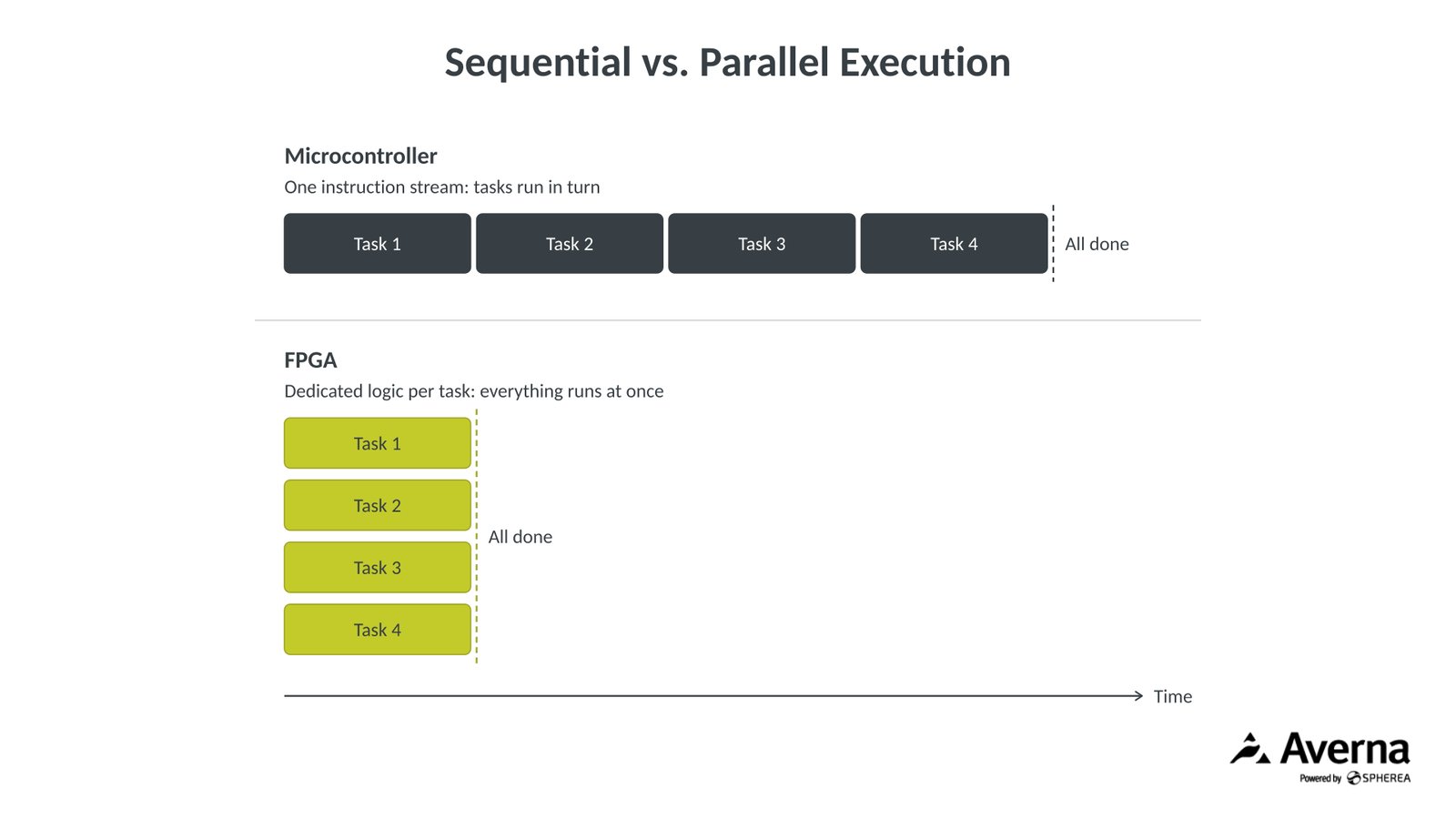
A microcontroller is a small computer on a chip. It executes firmware instructions one after another, which makes it inexpensive and very power-efficient. While dedicated peripherals can handle many tasks independently, meeting strict timing requirements is generally more challenging than with dedicated hardware.
An ASIC is custom silicon designed for a single job. It delivers the best performance and power efficiency of the three, along with the lowest unit cost at high volume. However, design costs and the cost of creating the semiconductor photomasks are high, and development takes months. This in addition to a frozen design, so any errors or changes after fabrication means a do-over.
An FPGA gives you a bit of both. Like an ASIC, it runs operations in massive parallelism with deterministic timing. Like a microcontroller, it can be changed after deployment, simply by loading a new bitstream. That combination makes it the default choice for low to medium volumes, evolving designs and prototypes of future ASICs.
| Criteria | Microcontroller | FPGA | ASIC |
|---|---|---|---|
| Execution | Sequential instructions | Parallel hardware | Parallel hardware |
| Reconfigurable after production | Firmware only | Yes | No |
| Timing | Depends on software load | Deterministic | Deterministic |
| Upfront cost | Low | Low to moderate | High |
| Unit cost at high volume | Low | Moderate to high | Lowest |
| Typical use | Control tasks, embedded systems | Real-time processing, test systems, prototyping | Mass-produced products |
How Is an FPGA Programmed?
Programming an FPGA means defining how the circuit should behave. Most engineers do it in a hardware description language such as VHDL or Verilog, although high-level synthesis tools accept C or C++ and model-based tools can generate HDL straight from MATLAB or Simulink.
From there, the toolchain simulates the design, synthesizes it into logic, maps it onto the chip’s logic resources, places and routes it on the fabric, and finally produces the bitstream.
With LabVIEW FPGA, engineers draw the logic as block diagrams instead of writing HDL, which shortens the learning curve for test engineers already familiar with LabVIEW. The discipline stays the same, though: resource usage and timing still need close attention, and structuring that code into reusable modules pays off quickly on larger projects.
Applications of FPGAs
FPGAs are mostly used when systems need to process large volumes of data in real time. Four capabilities explain most of their applications:
- Parallel I/O operations. An FPGA can read and drive hundreds of signals simultaneously, each with its own dedicated logic, instead of polling them one by one like a processor.
- Data acquisition. Paired with analog-to-digital converters, an FPGA captures and pre-processes high-speed data streams before passing them to a host computer, ensuring that no sample is lost.
- Specialized computations. Algorithms such as filtering, FFTs or encryption run directly in hardware, often much faster and with more predictable timing than in software.
- Custom processors. Engineers can build a processor architecture tailored to one task, or implement a soft-core processor inside the fabric to handle control functions alongside the dedicated logic.
These capabilities show up across many sectors, a few of which rely on FPGAs more than others.
Machine Vision and Imaging
A camera on a production line can generate more pixels per second than a processor can handle. An FPGA placed between the sensor and the host can correct and analyze each frame as it streams in, so that only the relevant results reach the software. That is why FPGAs fit so well into machine vision systems where inspection decisions have to keep pace with the line. The same low-latency logic applies to immersive displays, where even a small delay between head movement and image update breaks the experience, a challenge explored in FPGA-based virtual reality applications.
Telecommunications and Semiconductors
Wireless standards evolve faster than custom silicon can be designed, so telecom engineers rely on FPGAs to process radio signals in real time, from 5G base stations to radar systems. Chip designers use them in a similar spirit, running ASIC or System-on-Chip (SoC) designs on FPGA platforms months before the first wafer is back. Once the silicon arrives, FPGAs show up again in semiconductor testing programs, generating the high-speed digital patterns that device verification requires.
Why Do Test and Measurement Systems Rely on FPGAs?
If the timing on a test system drifts, you can no longer tell whether a failure comes from the product or from the bench...and that is exactly what a test system is for. When it triggers an acquisition or reacts to an event on the device under test, it has to do it exactly the same way every time, regardless of what else is going on. FPGAs give you that guarantee, because logic built in hardware never waits for an operating system or fights other tasks for processor time.
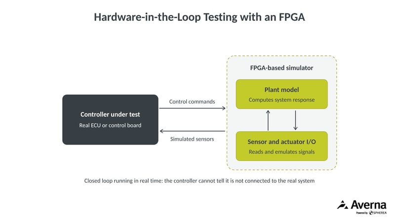
Hardware-in-the-loop testing is a good example. To validate a controller before the real system exists, the test bench has to simulate sensors and actuators fast enough that the controller cannot tell the difference. FPGAs run those models at loop rates a processor alone cannot sustain, which is why they sit at the core of many HIL solutions. The same applies to vision inspection systems, where image processing has to keep up with production speed.
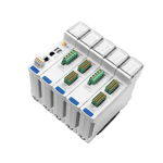 We use the same principle in our own instruments. In the PQA-Flex power quality analyzer, input modules digitize the signals and send their data over a digital backplane to an FPGA on the CPU module. The FPGA receives and processes those streams in real time, while a separate real-time controller runs the meter firmware.
Splitting the work this way lets the analyzer scale to high channel counts without compromising measurement timing.
Electronics and PCB Testing
On electronics production lines, FPGA-based instruments drive the digital stimuli and capture the responses that functional testers rely on. They can generate complex patterns, emulate communication protocols and check timing at speeds that would be out of reach for software-driven instruments. Our test systems use them alongside other PCB test methods, including in-circuit testing, to cover both the structural integrity of a board and its behavior under real operating conditions.
How Do FPGAs Speed Up Prototyping?
A new algorithm rarely works perfectly the first time it is implemented with real signals. With FPGA-based engineering prototyping, engineers can run it on actual hardware and refine it in days, instead of waiting months for a custom chip. Since the FPGA can be reprogrammed as often as necessary, most iterations only cost a new bitstream. FPGAs are therefore an ideal platform for proof-of-concept projects and for programs whose specifications are still evolving. Thinking about design for testability at this stage also saves a lot of headaches once the board heads to production.
That said, FPGA prototyping is not free of hardware iterations. In ASIC prototyping, an off-the-shelf FPGA board may not meet the requirements, so a custom FPGA board may be necessary, and changes in specifications can require PCB respins if the existing hardware cannot support them. Even accounting for these additional hardware iterations, FPGA prototyping is generally far less expensive than an ASIC fabrication run. It also has limits: an FPGA prototype does not necessarily reproduce ASIC timing, power consumption or physical implementation characteristics. It is particularly valuable for functional validation, but it does not replace ASIC implementation and sign-off verification.
A 5G Prototype Built on More Than 50 FPGAs
We saw this firsthand during a multi-year 5G project for a Silicon Valley technology company. The client needed a prototype it could take into field trials, but its design existed only as MATLAB scripts and system drawings, and its team had little experience with NI hardware. Meeting the real-time processing requirements called for more than 50 FPGAs working together.
We recommended building the system on a large NI platform combining USRP software-defined radios with high-speed serial FPGA boards. Working closely with the client’s design team, we ported its MATLAB models onto the USRP and continuously implemented new versions of the algorithms as they evolved, optimizing the hardware and software along the way. Our engineers also took part in the field trials.
Running the design on real hardware this early exposed major design and conceptual flaws while they were still inexpensive to fix. The client reached a working prototype much faster than a custom hardware approach would have allowed, and avoided investing in unnecessary hardware.
Need FPGA Expertise for Your Next Project?
FPGAs sit at the meeting point of hardware and software, and getting the most out of them takes fluency in both. A design that looks right in simulation still must hold its timing on real silicon and remain testable once it reaches production.
At Averna Powered by Spherea, FPGA work runs through much of what our engineers do, from LabVIEW FPGA development and prototyping to the production test systems that validate electronics on the line. Whether you need to turn a MATLAB model into a working prototype or build a test system with true real-time performance, our test engineering teams can help you get there faster.

You may also be interested in…

What would you choose between machine vision and human vision for inspection?


